


Texas Instruments SN65DSI85/SN65DSI85-Q1 DSI to FlatLink Bridge
Texas Instruments SN65DSI85/SN65DSI85-Q1 DSI to FlatLink™ Bridge features a dual-channel MIPI D-PHY receiver front-end configuration with four lanes per channel operating at 1Gbps per lane and a maximum input bandwidth of 8Gbps. The bridge decodes MIPI DSI 18bpp RGB666 and 24bpp RGB888 packets. The device also converts the formatted video data stream to a FlatLink™ compatible LVDS output operating at pixel clocks operating from 25MHz to 154MHz, offering a Dual-Link, Single-Link LVDS, or two Single-Link LVDS interface(s) with four data lanes per link. The SN65DSI85/SN65DSI85-Q1 is well suited for WQXGA (2560 × 1600) at 60 frames per second and 3D Graphics at WUXGA and True HD (1920 × 1080) resolutions at an equivalent 120 fps with up to 24 bits-per-pixel. Partial line buffering is implemented to accommodate the data stream mismatch between the DSI and LVDS interfaces. The Texas Instruments SN65DSI85-Q1 devices are AEC-Q100 qualified for automotive applications.
Features
- Implements MIPI D-PHY version 1.00.00 physical layer front-end and display serial interface (DSI) version 1.02.00
- Dual-channel DSI receiver configurable for one, two, three, or four D-PHY data lanes per channel operating up to 1Gbps per lane
- Supports 18bpp and 24bpp DSI video packets with RGB666 and RGB888 formats
- Suitable for 60fps WQXGA 2560 × 1600 resolution at 18bpp and 24bpp color, and WUXGA 1920 × 1200 resolution with 3D graphics at 60fps (120fps equivalent)
- MIPI® front-end configurable for single-channel or dual-channel DSI configurations
- FlatLink™ output configurable for single-link or dual-link LVDS
- Supports dual-channel DSI ODD or EVEN and LEFT or RIGHT operating modes
- Supports two single-channel DSI to two single-link LVDS operating mode
- LVDS output clock range of 25MHz to 154MHz in dual-link or single-link mode
- LVDS pixel clock may be sourced from a free-running continuous D-PHY clock or external reference clock (REFCLK)
- 1.8V main VCC power supply
- Low-power features include shutdown mode, reduced LVDS output voltage swing, common mode, and MIPI® ultra-low power state (ULPS) support
- LVDS channel swap, LVDS pin order reverse feature for ease of PCB routing
- ESD rating ±2kV (HBM)
- Packaged in 64-pin 5mm x 5mm nFBGA (ZXH)
- –40°C to 85°C temperature range
Applications
- PC & notebooks
- Tablets
- Connected peripherals & printers
Datasheets
Functional Block Diagram

Related Development Tools
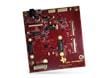
Texas Instruments SN65DSI85EVM LVDS-Brücken-Evaluationsmodul (EVM)
Die PCB, wurde entwickelt, um Kunden bei der Implementierung der SN65DSI85 in die Systemhardware zu helfen.
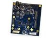
Texas Instruments SN65DSI8xQ1-EVM LVDS-Brücken-Evaluationsmodul
Entwickelt, um Kunden bei der Implementierung der SN65DSI83, SN65DSI84 und SN65DSI85 in der Systemhardware zu helfen.
Veröffentlichungsdatum: 2017-07-21
| Aktualisiert: 2022-06-06